Customer success
November 10, 2025

Plug-and-Play connector for highly efficient fiber-to-PIC coupling with sub-dB losses

SEM image of ultra-compact 3D splitters
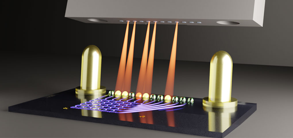
Illustration of a novel plug-and-play fiber-to-chip connector: a photonic integrated circuit (blue) couples light through 3D-printed total internal reflection micro-optics (TIR) to a polished multi-fiber termination push-on fiber array (MTP). 3D-printed alignment pins on the chip ensure precise, self-aligned optical connection. Image: © Erik Jung, Heidelberg University.

Photonic chips hold enormous potential for next-generation computing and communication, yet their deployment is hindered by complex, costly, and alignment-sensitive interfacing. Researchers at Heidelberg University have now demonstrated a plug-and-play fiber-to-chip connector, replacing active alignment steps with a passive mechanical-microoptical interlock that enables low-loss optical coupling simply by insertion. The connector, produced through aligned 3D microprinting directly on the chip, achieves passive, broadband, and sub-dB loss coupling in under three minutes packaging time per port. This new concept paves the way for scalable, alignment-free photonics packaging in PIC-based systems.

Photonic integrated circuits (PICs) are reshaping fields such as high-speed communications, quantum technologies, and neuromorphic computing by offering unprecedented bandwidth, ultra-low latency, and superior energy efficiency compared with conventional electronic chips. Fabricated with lithographic techniques similar to those used for electronic chips, PICs integrate essential optical components like waveguides, modulators, and detectors on a single platform to guide and process light with high precision and stability.

Yet optical interfacing remains one major bottleneck: Coupling light in and out of the chip for data transfer typically requires fibers positioned with micrometer precision relative to narrowband grating couplers. Even state-of-the-art fiber-array-to-chip coupling still relies predominantly on active alignment, a process that remains time-consuming, costly, and difficult to scale in production environments.

Researchers at Heidelberg University have now addressed this challenge with a scalable plug-and-play fiber-to-chip connector fabricated by aligned high-precision 3D microprinting. The new approach enables self-aligned, broadband and low-loss optical coupling, replacing complex alignment setups with a simple insertion-locked connection.

Integrated optical and mechanical interface

The researchers developed a novel packaging concept that uses additive manufacturing to achieve optical coupling and mechanical alignment. Using multi-fiber termination push-on fiber arrays (MTP) with standardized alignment pinholes, the team 3D-printed the matching counterpart directly onto the photonic chip by Two-Photon Polymerization (2PP). Coupling is realized via total internal reflection (TIR) couplers that focus and redirect light from the on-chip waveguides into the fibers providing broadband, and low-loss coupling.

The concept was validated on a 16-input-port photonic tensor core for neuromorphic computing, demonstrating self-aligned fiber coupling with sub-dB insertion losses and nearly wavelength-independent performance. By combining a mechanical interlocking mechanism with optical coupling, the team achieved a scalable and manufacturing-ready connector design – a significant step toward alignment-free packaging for large-scale PIC systems.

Scalable packaging solution for photonic integration

The new connector concept directly addresses a central challenge in photonic integrated circuit (PIC) packaging, achieving broadband, low-loss, and scalable optical interfacing. By eliminating active alignment, it enables automated, reproducible, and cost-efficient manufacturing, paving the way for volume production of advanced PIC-based systems.

Fully compatible with hybrid electronic–photonic integration, this approach supports modular and reconfigurable architectures required for quantum computing platforms, neuromorphic processors, and optical sensing systems. As a mass-manufacturable, passive packaging solution, it marks an important step toward practical large-scale deployment of next-generation photonic technologies in communications and computing.

Driving results with aligned high-precision 3D printing

Fabricating the low-loss, broadband, plug-and-play connector required meeting two key demands: mechanically stable alignment structures and a transparent, infrared-compatible material for optical coupling. These challenges were addressed with the Quantum X align system, whose high-precision Direct Laser Writing (DLW) process enables high-resolution 3D printing with nanometer-level alignment accuracy across different feature scales. 

In a first DLW step focusing total internal reflection (TIR) couplers, each about 30 µm in height, were printed directly on the photonic chip. Using the Small Feature Print Set allows the fabrication of sub-micrometer optical structures in IP-Dip2, a transparent, infrared-compatible resin. With automatic marker-based alignment, the couplers were precisely positioned relative to the on-chip waveguides, while Two-Photon Grayscale Lithography (2GL®) ensured excellent optical performance by producing each coupler with smooth, accurately shaped surfaces in less than one minute.

Design of the 1×4 3D MMI (multimode interference) splitter
MTP cable plug-in process onto a PIC: The pre-alignment structure supports the cable’s weight and guiding pins enable micron-precise alignment. © E. Jung, J. Römer, Heidelberg University
Microscope image of a silicon nitride PIC coupled via focusing TIR micro-optics
Microscope image of a silicon nitride PIC coupled via focusing TIR micro-optics: the 12×2 MTP fiber array is precisely positioned using 3D-printed alignment pins fabricated by Two-Photon Grayscale Lithography (2GL®). © Erik Jung, Heidelberg University
Graph of finite Element Frequency-Domain (FEFD) simulation
Finite Element Frequency-Domain (FEFD) simulation showing normalized optical power propagation within the total internal reflection (TIR) coupler structure. © Erik Jung, Heidelberg University
SEM image of a silicon nitride waveguide backloop with printed TIR micro-optics
SEM image of a silicon nitride waveguide backloop with printed TIR micro-optics: the micro-optics are fabricated with sub-micrometer precision relative to the on-chip waveguides using marker-based alignment. © E. Jung, M. Ulanov, Heidelberg University
Graph with the comparison of the coupling efficiency by the transmission spectra of a 16-input-port photonic tensor core between 1500 and 1600 nm.
A comparison of the coupling efficiency is shown by the transmission spectra of a 16-input-port photonic tensor core between 1500 and 1600 nm. The plug-and-play connector (color per port; see legend) is compared to a state-of-the-art grating coupler (blue). © Erik Jung, Heidelberg University

In a second DLW step on the same chip, the Large Feature Print Set was used to fabricate the mechanical components that form the plug-and-play interface. These taller structures, up to 2 mm in height, were automatically aligned relative to the photonic structures. 

Overall, the packaging for each optical port was completed in less than three minutes, demonstrating not only the scalability of the connector concept but also the reproducibility and precision enabled by Quantum X align’s multi-scale 3D printing technology.
 

Would you like to find out more about this inspiring project? Then read the open access publication in Science Advances, Volume 11.

Access a curated database of over 2,100 peer-reviewed research projects enabled by Nanoscribe’s high-precision 3D microfabrication technology. Explore how researchers worldwide are applying our technology in micro-optics, life sciences, microfluidics, and beyond. Register for free to evaluate its relevance for your own applications and development goals.

Login Register
Contact us
Close

It's your choice

Cookies help us to better understand you as a visitor and to provide you with a better experience.

It's your choice
Cookies help us to better understand you as a visitor and to provide you with a better experience.
Legal Notice Privacy Policy
Accept all Individual Settings